Electro-optic modulation converts an electrical waveform into a controlled change in light. That principle serves data transmission, precision sensing, microwave photonics, and test instrumentation, but each field values a different output. Accordingly, they start with the physical function required by the system rather than assuming that a fast modulator is automatically suitable for every optical task.
Communication teams focus on data rate, reach, extinction, linearity, and power. Sensing teams may care more about phase noise, chirp quality, stability, and calibration. Test systems need flexible control, known reference planes, and repeatable behavior.
Shared device technology can shorten development when the package and operating limits remain compatible with these different priorities. Program teams maintain separate requirement matrices for each market so that a shared chip does not inherit contradictory limits or unnecessary certification work.
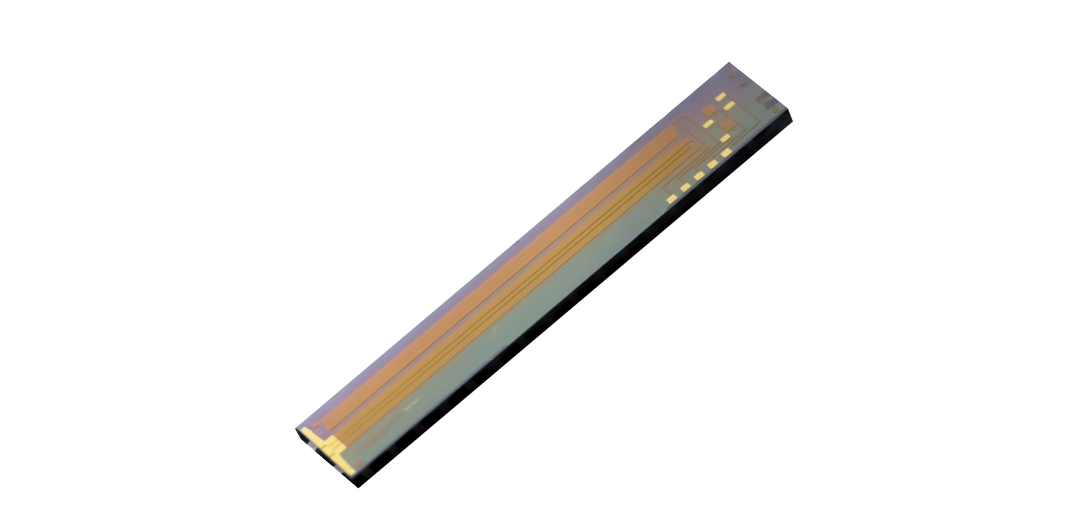
The available portfolio of TFLN chips includes multi-channel direct-detection devices, coherent IQ circuits, and a bare intensity-modulator die with bandwidths up to 110 GHz. Across those cases, they examine how one material platform may support several applications, while keeping device selection tied to measured system behavior, packaging responsibility, and production readiness.
One Device Principle Supports Several System Functions
In communication, an electro-optic modulator shapes light for direct or coherent detection. Direct links may require rapid intensity levels and high extinction, whereas coherent transmitters combine amplitude and phase.
They translate modulation format and symbol rate into bandwidth, drive, and linearity limits, then confirm performance with the actual laser, driver, fibers, and receiver path.
TFLN chips can also support sensing through controlled phase or frequency behavior. FMCW LiDAR, interferometric instruments, and microwave-photonic systems may use modulation to create chirps, sidebands, or phase shifts.
Their assessment includes frequency noise, waveform linearity, timing, optical power, and environmental stability because small errors can translate directly into range or measurement uncertainty. Test equipment uses modulation as a stimulus rather than as the final product output.
Engineers may need controllable amplitude, phase, wavelength-sideband structure, or high-speed conversion to validate another device. They require access to settings, monitoring, calibration data, and trigger behavior so that the modulator produces a known input rather than a waveform observed on one instrument.
Application Requirements Change the Meaning of Performance
For direct-detection communication, TFLN chips listed for 800G, 1.6T, and 3.2T show how bandwidth, differential voltage, insertion loss, and extinction interact. Multi-channel integration can reduce component count, but lane balance and coupling yield matter. They compare system energy and optical margin across the full engine instead of ranking chips by bandwidth alone.
A coherent electro-optic modulator adds nested paths and bias points. The listed 70 GHz PDMIQ device targets 800G and 1.6T ZR formats with loss below 7 dB, differential half-wave voltage below 4.5 V, and extinction above 25 dB.
They evaluate quadrature balance, linearity, bias-control range, and package symmetry under representative large-signal operation. For sensing or testing, a bare 110 GHz intensity die may provide integration freedom. Its listed loss below 5 dB, half-wave voltage below 3 V, and extinction above 20 dB are useful inputs, yet their package design must preserve them.
Fiber coupling, RF launch, thermal stress, and fixture access become part of the engineering responsibility transferred with the bare die. Calibration ownership is assigned explicitly, including who maintains reference waveforms, correction files, and software after the original development engineers move to other projects.
Integration and Qualification Decide Whether Reuse Is Practical
Using TFLN chips across several product families can create shared models, packages, and test methods, but qualification cannot be copied blindly. Communication deployments may emphasize lifetime and network availability; sensing may require vibration, temperature range, and calibration stability; laboratory instruments may prioritize configurable access.
They document what evidence transfers and where application-specific testing begins. Control requirements vary because an electro optic modulator requires controls that match its role.
Data transmitters may rely on firmware-managed bias and alarms, sensing systems may require synchronized waveform generation, and test platforms need user-visible states.
They define interfaces, telemetry, recovery behavior, and error reporting early so that control electronics do not become an afterthought that limits the optical device. Supply-chain planning covers wafer fabrication, die screening, packaging, calibration, and failure analysis.
They review process capacity and lot traceability because specialized applications may initially use low volume but later demand stable repeatability. A common platform is useful when suppliers can preserve performance while supporting different package options and qualification regimes.
Business cases include development tooling and qualification reuse, revealing whether cross-application commonality produces genuine savings or shifts effort between departments. Communication, sensing, and testing all use electrical control of light, yet they convert that capability into different forms of value.
The correct modulator is defined by the waveform, operating environment, interfaces, and evidence needed for the finished product. Common technology simplifies development after those application boundaries have been made explicit.
Their evaluation therefore combines electro-optic measurements with link tests, sensing accuracy, calibration behavior, environmental work, and manufacturing trials. They compare complete operating windows rather than isolated typical values. This reveals whether a platform can genuinely serve multiple markets or merely produce early-stage results under one carefully selected condition.
Communication, sensing, and testing apply electro-optic modulation under different waveform and qualification conditions. Buyers may evaluate Liobate chips in separate requirement matrices for each use. A shared technology should be adopted where it reduces development effort without obscuring application-specific limits.
